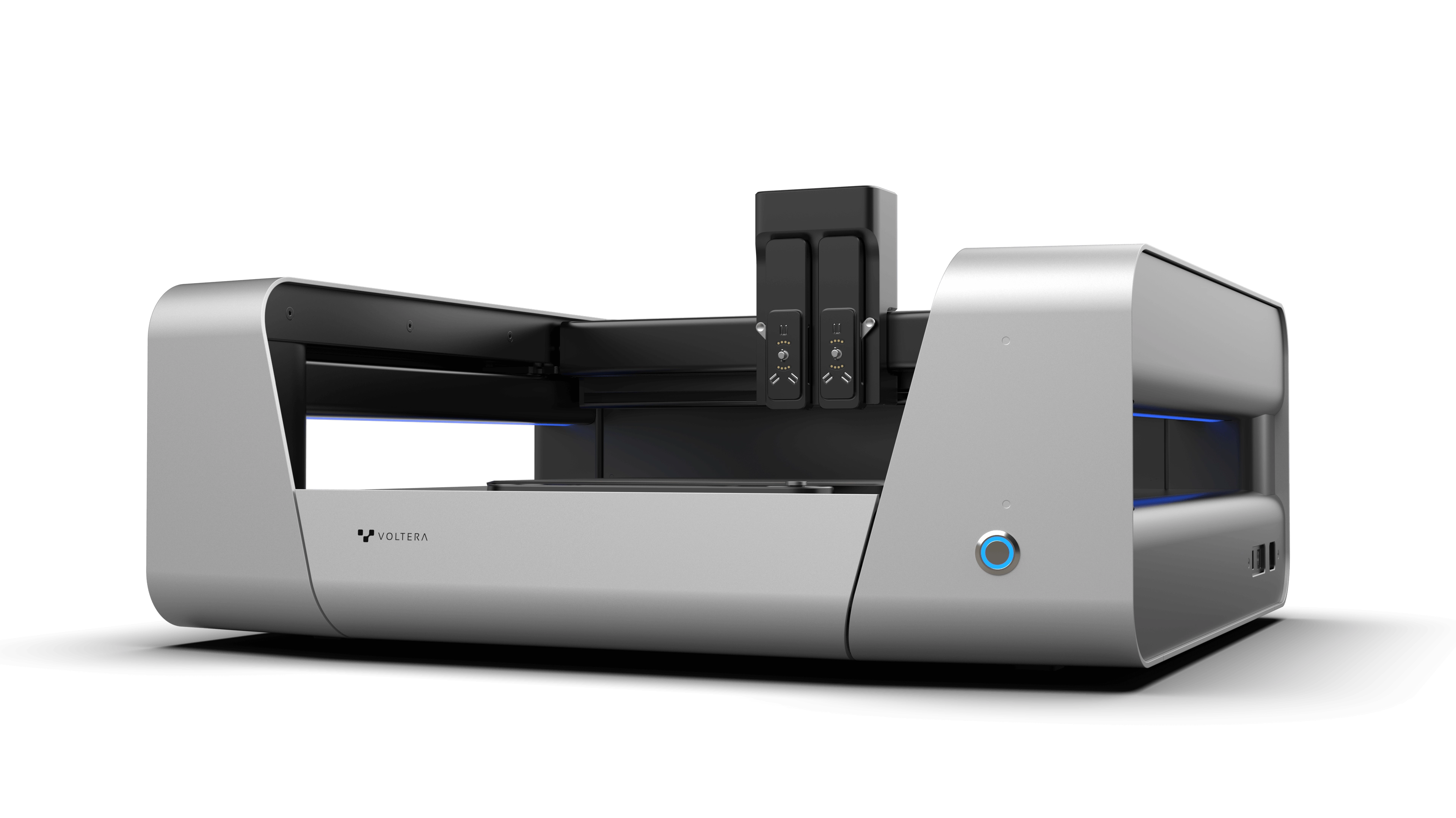
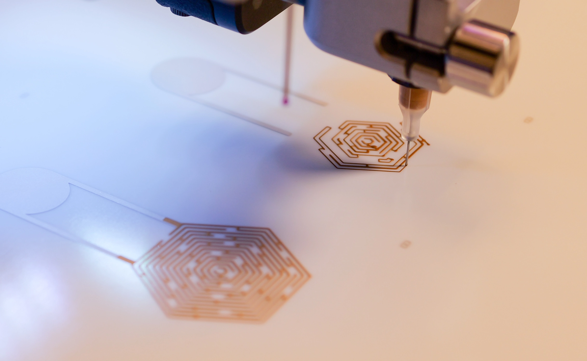
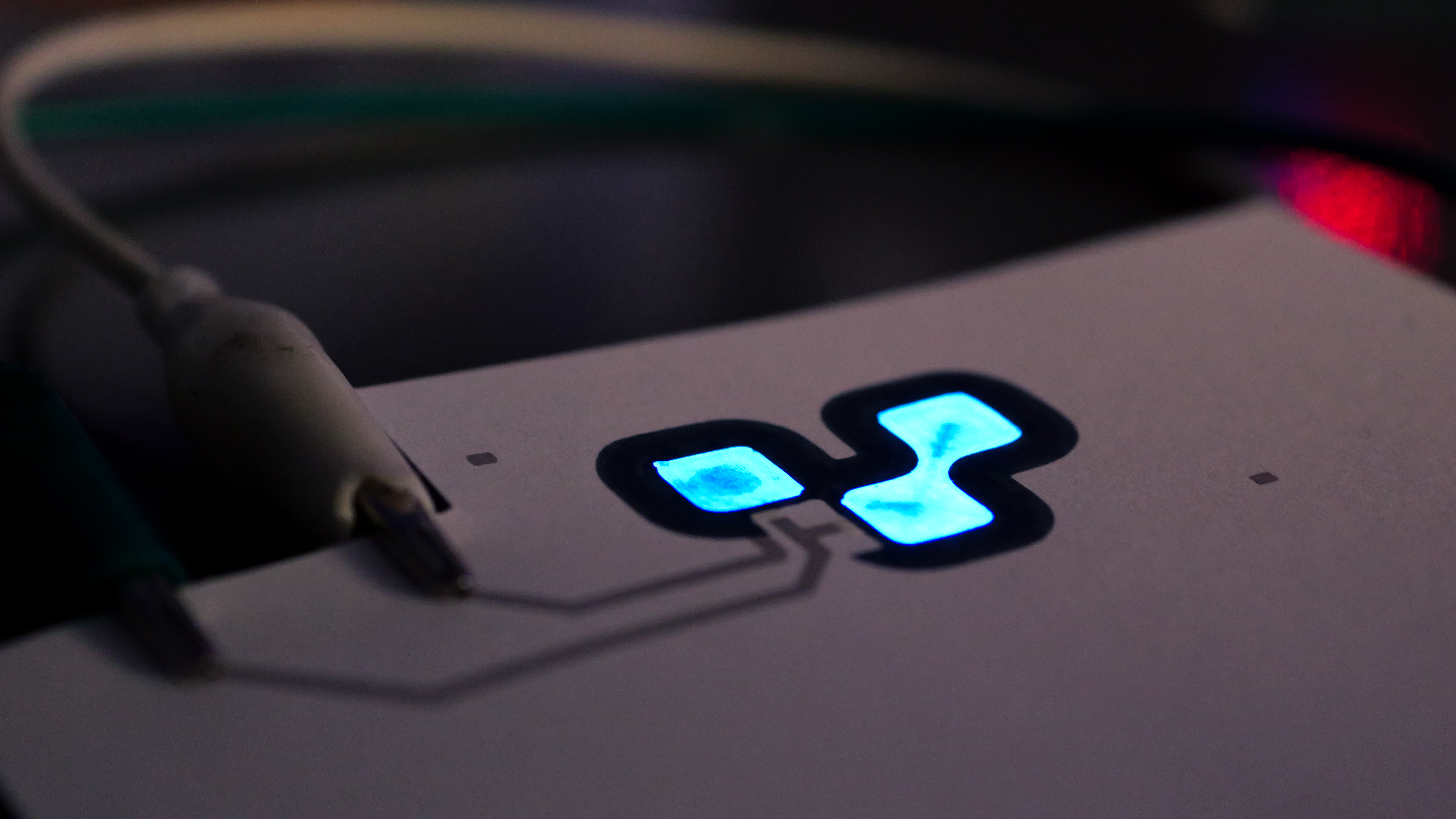
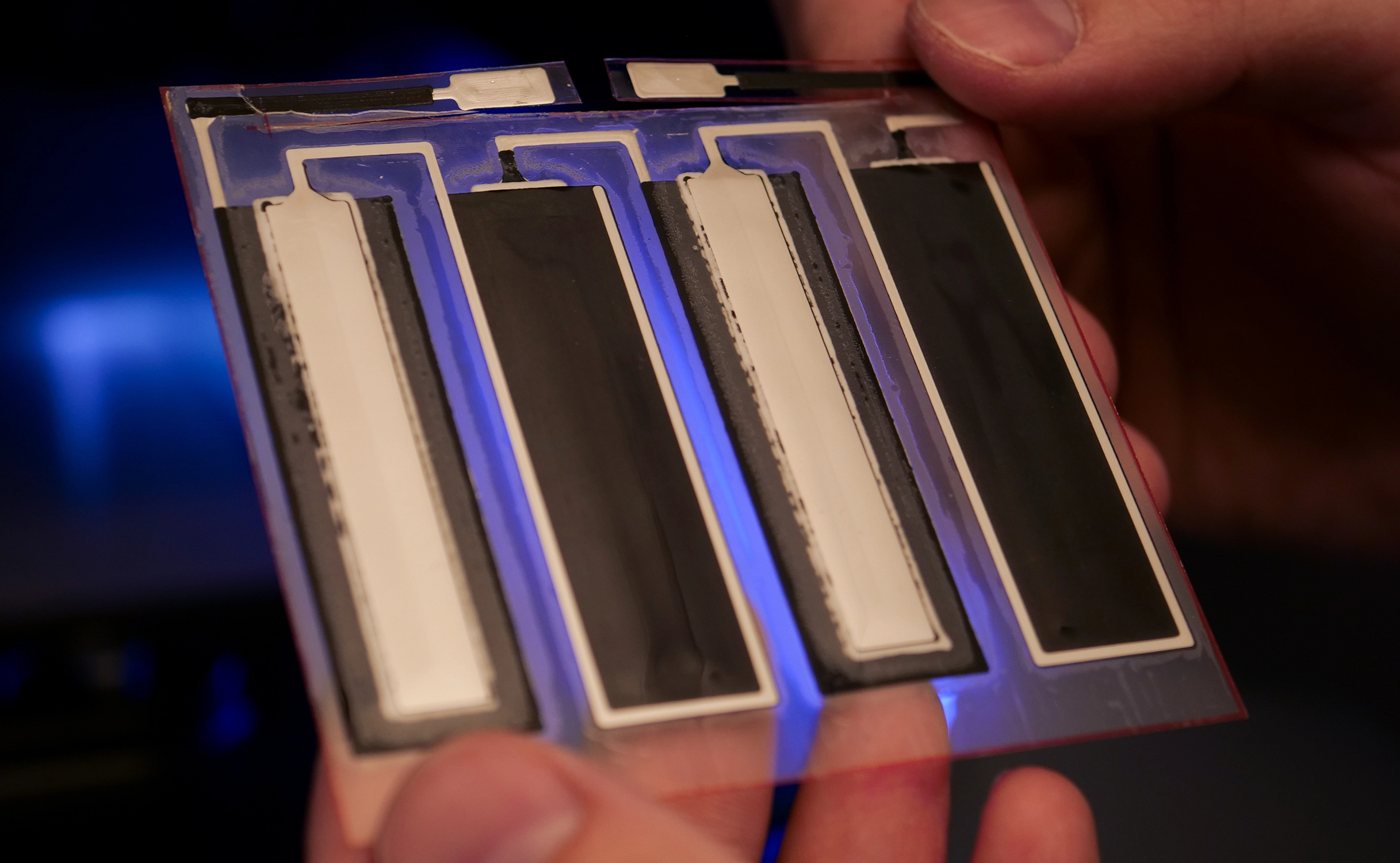
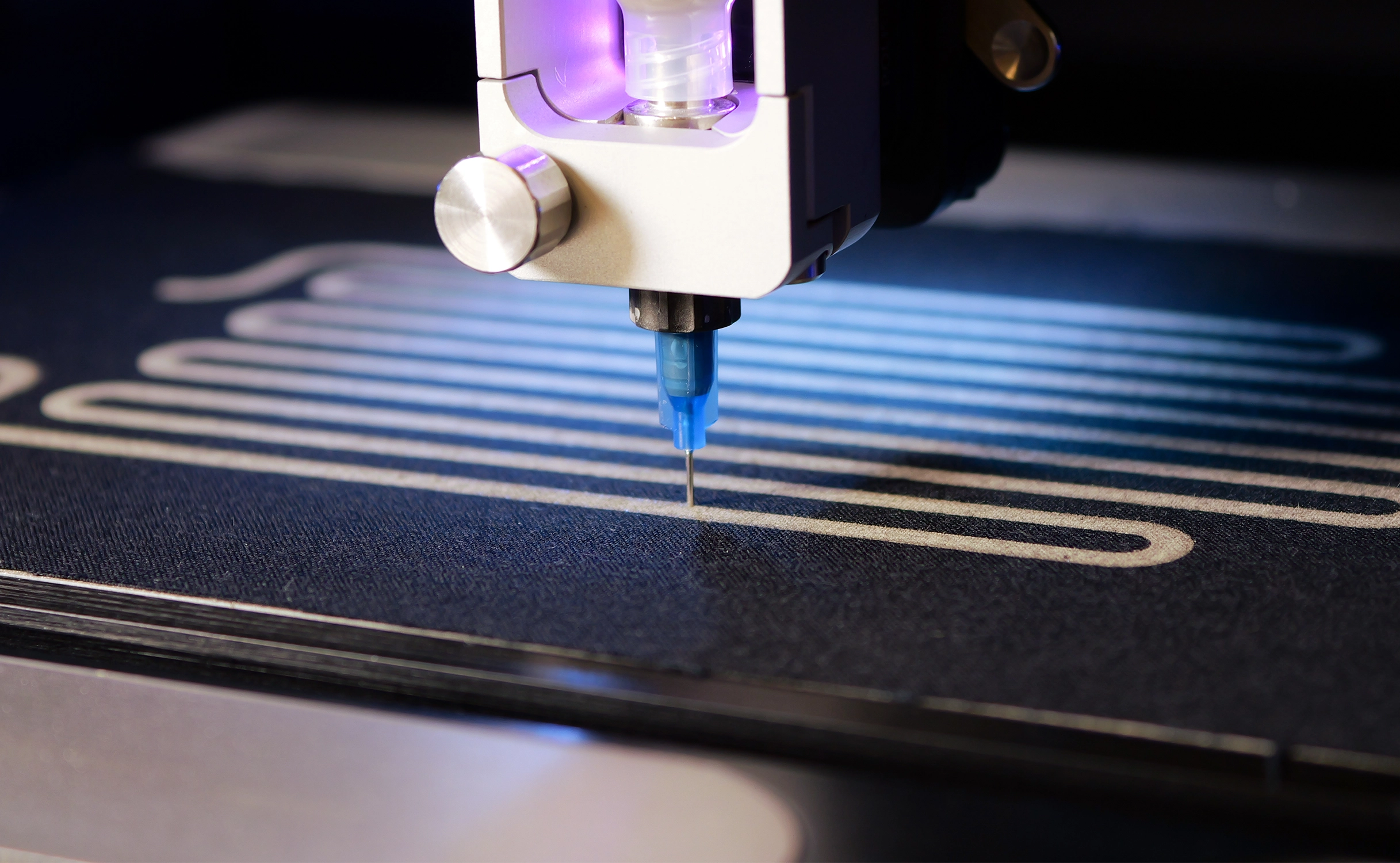
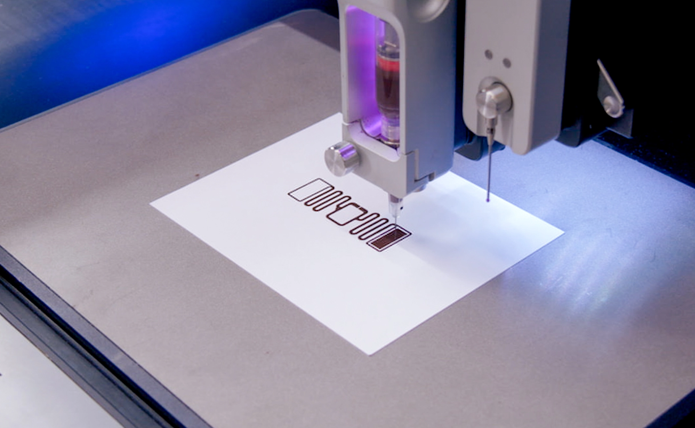
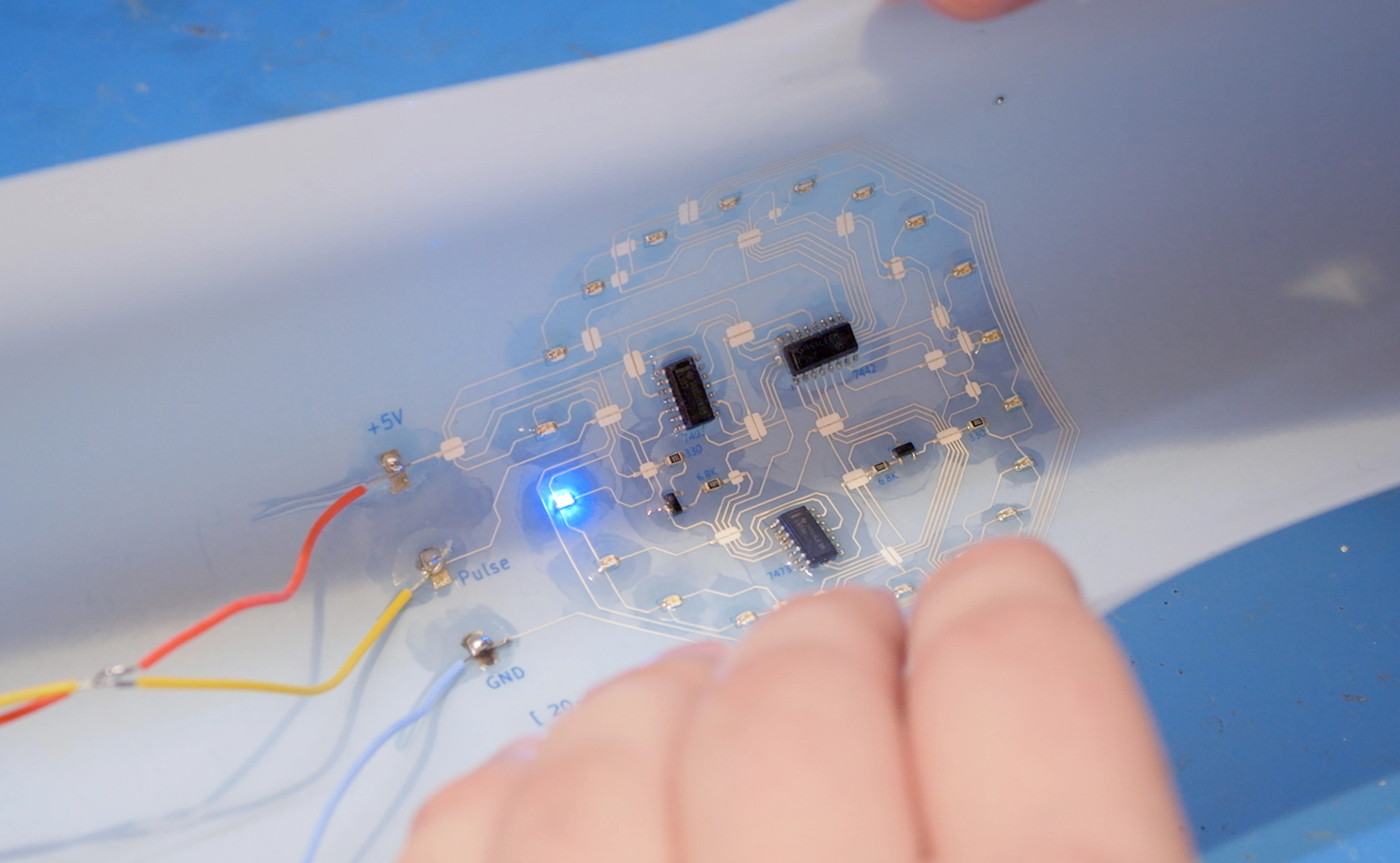
Voltera NOVAVoltera NOVA – a modular dispensing system for printed electronicsAutomated platform for direct printing (dispensing) of functional materials – conductive inks, dielectrics and biocompatible materials – on rigid, flexible and non-standard substrates, with closed-loop pressure control and camera-assisted machine vision. Ask for a quote See specifications ↓220 × 300 mmPrint areafrom 100 µmLine widthup to 4Layers in a stack-up17 µm/pxCamera resolution Why NOVAOpens up new possibilities in printed electronicsOpen new possibilitiesDirect printing from functional materialsApplications beyond classic PCBs and siliconFlexible electronics, sensors, cells, antennas, textilesAccelerate R&DNo tooling, waste, or cleaningUp to 90% faster design iterationUp to 96% less material used in the R&D phaseComplete material freedomMaterials with a viscosity of 1000–1000000 cPConductive, dielectric, biocompatible and other functional materialsPrinting on glass, polymers, paper, fabrics and flexible substratesTechnical SpecificationsVoltera NOVA parametersPrinting technologyDirect Ink WritePressure controlClosed loopPrint area220 × 300 × 40 mmMinimum line widthfrom 100 µm*XYZ resolution2,5 µm × 7 µm × 1,25 µmPositioning accuracy±20 µmMaximum number of layersup to 4 in stack-up**Syringe capacityup to 2,5 mlMaterial viscosity1000 – 1,000,000 cPMaterial temperatureup to 40°CWorktableVacuum table, M5 mesh 40×40 mm, up to 30 mm substrate heightCamera/machine vision8 MP, resolution up to 17 µm/px, AR overlayDimensions / weight675 × 605 × 345 mm / approx. 35 kgPower100-240 VAC, 50/60 Hz, 221 WCommunicationUSB-A 2.0 + USB-A 3.0 + Ethernet + Wi-Fi (dongle included)* depending on material and nozzle ** designs with more layers possible after consultation with VolteraWhat's in the setNOVA printerSmart dispenserSmart probeVacuum TableConductive InkPressure Sensor – 3 pcs.Anchor Mount – 4 pcs.Swivel Mount – 4 pcs.Wing screws – 4 pcs.Clear Cartridges – 4 pcs.UV Blocking Cartridges – 4 pcs.Luer Couplers – 4 pcs.Tip Cap – 3 pcs.Pistons – 16 pcs.Subrex 100 µm nozzles – 4 pcs.Subrex 150 µm nozzles – 4 pcs.Subrex 225 µm nozzles – 4 pcs.PET substrate sheets – 10 pcs.Polyimide (PI) substrate sheets – 2 pcs.TPU backing sheets – 5 pcs.Nozzle WrenchWi-Fi adapterCleaning brushPower cablePowerEthernet cable See more (21)▾ Catalog number: 1000400 complete set brand newApplication examplesFrom Medical Electrodes to Flexible PCBs ECG electrodesPrinting gold electrodes on flexible substrates for wearable medical devices monitoring heart function. Electroluminescent circuitsMultilayer EL structures – electrodes, dielectric and phosphor layers – printed sequentially on a single substrate. Magnesium-zinc batteriesPrinting flexible, biodegradable, next-generation energy cells for disposable and medical electronics. Printing on fabricsSmart textiles with printed heating elements, sensors and antennas – directly on the material. RFID tagsProduction of thin, lightweight RFID antennas and tags on flexible substrates for logistics and asset tracking. Flexible PCBsPrinting flexible circuits with LED components and interactive elements on thin polymer films.SoftwarePlan – Design Layer by LayerPlan is a browser-based Voltera application – no installation required, works on any operating system:Gerber file compatibilityUp to 4 layers in a single stackCentral library of materials with ready-made recipesGuided walk-throughs with instructional videosControlling the direction of tool paths (eliminating air pockets)Live chat support available in the appThe plan significantly shortens the learning curve – users create advanced projects in the first days of working with NOVA."My research focuses on developing flexible and stretchable sensors for wearable electronics. Using the Plan function, I can separate sensor elements, traces, and components into separate layers and remove unwanted toolpaths. The ability to change the direction of toolpaths has been most helpful – there are no air pockets, and the path width is very uniform."Nick LevinskiUniversity of WaterlooThe most important advantagesWhy R&D teams choose NOVANo tooling, waste or cleaningUp to 90% faster design iterationUp to 96% reduction in material costsNo molds, masks, or time-consuming equipment cleaningMaterial versatilityLine width from 100 µmMaterial viscosity: 1000 – 1,000,000 cPUp to 4 layers in one stackMaterial temperature up to 40°CSupport for various substratesRigid – threaded mounting grid M5, 40×40 mmFlexible – porous titanium vacuum tableUnusual – custom handles and fixturesMachine vision with ARBuilt-in camera 1920×1080Resolution up to 17 µm/pixel (depending on the substrate)Augmented reality overlay for pattern alignmentReal-time print quality controlPrecision and closed loopXYZ resolution: 2,5 µm × 7 µm × 1,25 µmPositioning accuracy: ±20 µmClosed-loop pressure feedbackTemperature-controlled dosingIntuitive softwarePlan browser app (no installation required)Gerber file compatibilityCentral library of materialsLive chat support in the appCustomer reviewsThey trusted NOVA“The NOVA interface is so user-friendly that I can confidently entrust our technicians with operating the machine – without the need for weeks of training.”Andrew BambachProduction Manager, ACI Materials“NOVA opens up applications that go beyond classic silicon electronics and PCBs – it enables us to print structures on substrates and from materials that would be unattainable with standard processes.”Gerd GrauDirector of the Electronics Additive Manufacturing Lab, York University"We print inks from carbon nanotubes, from which field-emitted electrons power our devices. NOVA allows us to iterate these structures at speeds unattainable in classical laboratory processes."Alex KashkinGraduate Researcher, Velásquez Group, MITFAQMost frequently asked questionsWhat materials can I print?NOVA supports materials with viscosities from 1000 to 1,000,000 cP – conductive pastes (silver, copper, gold, carbon), dielectrics, biocompatible materials, electrolytes and other functional materials.What surfaces can you work on?Rigid (M5 mounting grid), compliant and flexible (porous titanium vacuum table), and unconventional geometries (custom fixtures) – glass, PI/PET/TPU polymers, paper, fabrics.How many layers can be printed?Up to 4 layers in a single stack-up design with Plan software – ideal for EL structures, multilayer sensors and cells.What are the power requirements?Standard power outlet: 100–240 VAC, 50/60 Hz, 221 W. NOVA does not require a dedicated laboratory installation.Does the Plan require installation?No. Plan is a browser-based application – it works on any operating system, no downloads required. It supports Gerber files, and technical support is available via live chat within the app.Are there additional modules available?Yes – thanks to ports with kinematic clutches, quick replacement is possible: UV curing module, interchangeable dispensing heads and accessories for working with different syringe formats.Warranty and support24-month warranty, extendable to 60 monthsDuring the warranty period, we guarantee repair or replacement of the device, and if that's not possible, we'll provide a refund. An extended warranty of up to 60 months can be ordered from Voltera. Ask for a quote and availabilityDo you have any questions? Check Chemikonics Product FAQs. 2-year warranty included in the pricePossibility of extension to 5 years. ×Ask about the productVoltera NOVAAby wypełnić ten formularz, włącz obsługę JavaScript w przeglądarce.To complete this form, please enable JavaScript in your browser.First name and last name *e.g. John Smith Message content name E-mail address *e.g. jkowalski@domain.comMessage content *A place for your inquirySubmit